Top
Open Source Chip Design
Getting Started
Install Open Source Tools
- Integrating Jupyter Notebook in VS Code
- Setting Up Open Source Tools with Docker
- Seamless Host-Side Control of Docker
Try It Out
-
Generate Analog Layouts in VS Code
Initial version: Jun 19, 2024
Verified with Windows
Verified with MacOS
Recorded Video of Live Demo (5:10 ~ 22:25)
In 2024 Chipathon by the IEEE SSCS, the main theme is about playing around with Automatic Generation of Analog Layout framework developed by Mehdi Saligane’s research team from University of Michigan.
Its name is GLayout, one of the winners of 2024 IEEE SSCS Code-a-Chip travel grant awards in ISSCC 2024. The below picture was taken during ISSCC 2024 with Sadayuki Yoshitomi and Anhang Li, explaining GLayout to folks.

If you are interested in learning more of the open-source activities in IEEE SSCS, please check this post!
In this post, I am going to guide how to setup the GLayout using Python, under Jupyter Notebook in VS Code environment. The introduced method has some remarks as follows:
- Please check This Post for setting up Jupyter Notebook in VS Code
- This post assumes that you already have built the Jupyter Notebook environment in VS Code
- It is recommended to build the Docker environment by following This Post for the future usage of the tools
- This post is geared to those people who are not familar with terminal and github usages
Create a New Conda Kernel
For Windows
For MacOS
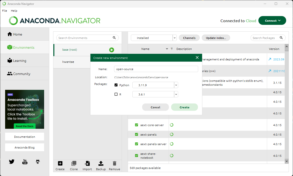
Open Anaconda Navigator app and go to Environments → Create to create a new kernel. I made a new kernel with the name of open-source in this example.
DO NOT SKIP THIS STEP!! Most of errors you encounter for following the procedures in this post arise when you try to reuse your existing kernel!
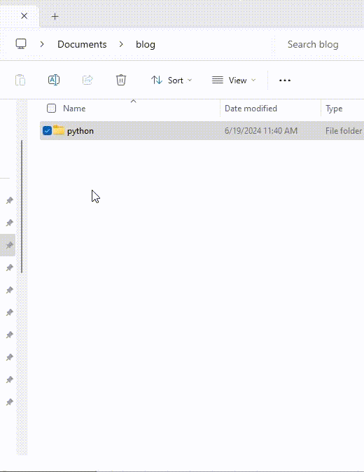
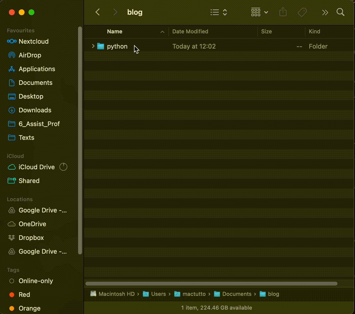
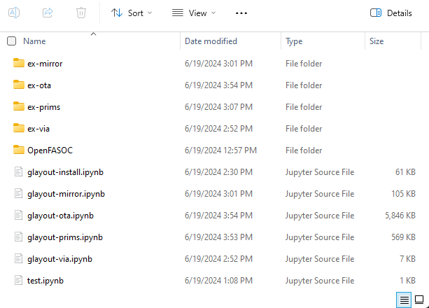
Make a new folder as you wish. I made a new folder python under Documents/blog/ path. Right click the folder, and open it with Code.
For Windows
For MacOS
(if you cannot see Visual Studio Code in Quick Actions, check this Video)
Open palette using
Ctrl + Shift + Pin WindowsCmd + Shift + Pin MacOS
create a new Jupyter Notebook, and select your new kernel. In this example, as I made a new kernel open-source, I selected it.
Save your Jupyter Notebook with shortcut
Ctrl + Sin WindowsCmd + Sin MacOS
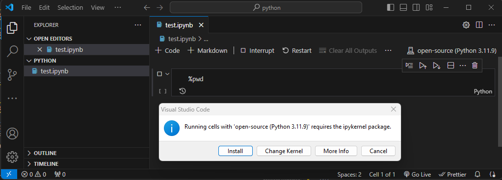
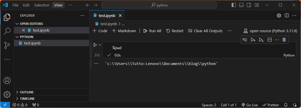
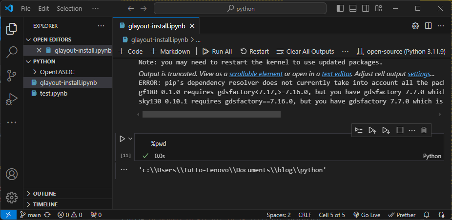
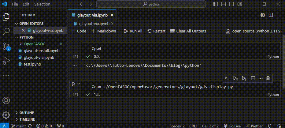
with the name test.ipynb as below screenshot, and run this simple code, %pwd, with shortcut Ctrl + Enter which is the same in both Windows and MacOS. The %pwd command tells you that what is your current directory. Then it will ask us to install package. Install it.
Upon installation, you should see the correct path as you made a new folder.
Install GLayout
First, we will build a Python code, glayout-install, for installing glayout in our new kernel.
After going through the method in this post, you will have the following files within your folder.
Git Clone the Repository
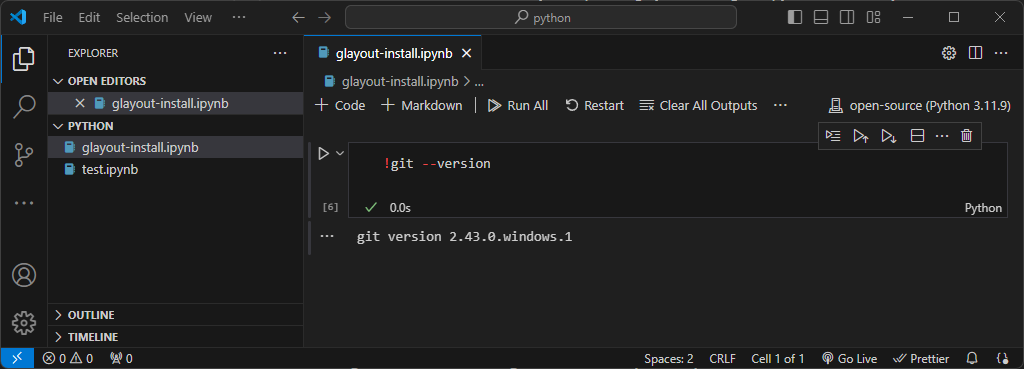
Make a new Jupyter Notebook with the name glayout-install as below screenshot, and run !git --version to check your OS has git installed. If it does not work, check This Post’s Git section.
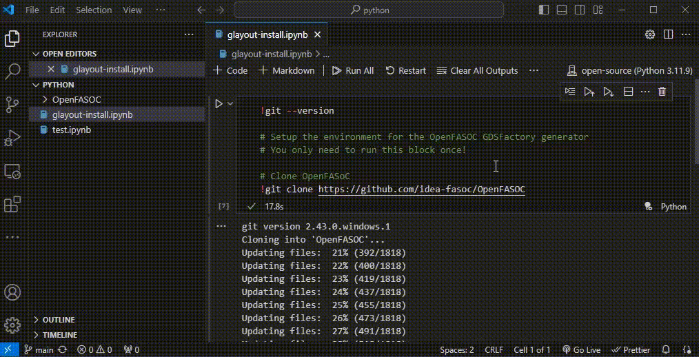
Now, run this git clone code to download the OpenFASOC repository.
!git clone https://github.com/idea-fasoc/OpenFASOC
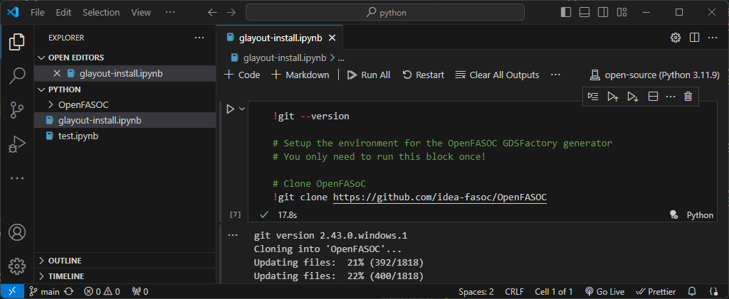
Upon completion, you should see a green check mark in your cell, and OpenFASOC folder on your left bar.
GLayout Package
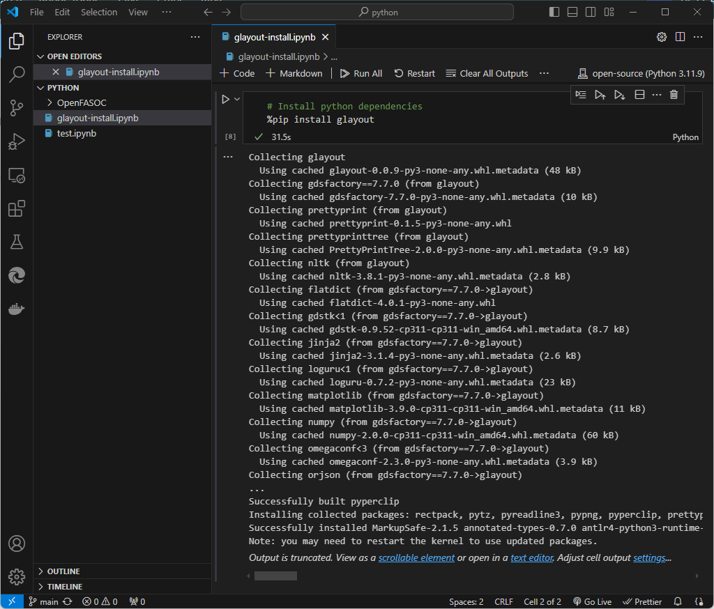
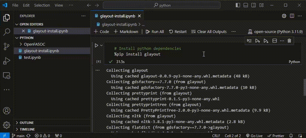
As you do not need to run this git clone code again, go down and make a new cell, and run the below code.
%pip install glayout
If it was successful, you can see the result like this.
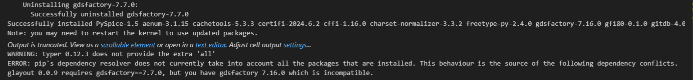
SKY130/GF180 PDK Packages
As the same flow, install sky130 and gf180 pdks
%pip install sky130 gf180
You will see the following error message which means that there is a version conflict in the usage of gdsfactory, but just skip it at the moment.
Remaining Packages
Install the following packages also in a different cell.
%pip install prettyprinttree
%pip install svgutils
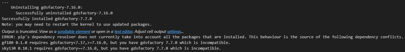
%pip install gdsfactory==7.7.0
Here, we installed gdsfactory 7.7.0 version but it again complains the version conflict . You can just ignore this error message.
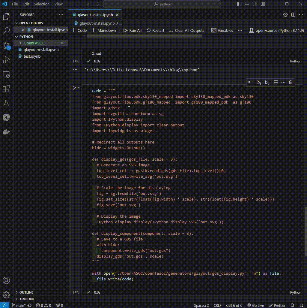
GDS Display Python Code
The next step of the installation is making a Python code for displaying the GDS file.
Before going through this step, make sure you are located in your top-level working directory by running %pwd. If not, click Restart icon to restart your kernel. In this example, it must be python folder as shown below.
Then run this code as a separate cell.
code = """
from glayout.flow.pdk.sky130_mapped import sky130_mapped_pdk as sky130
from glayout.flow.pdk.gf180_mapped import gf180_mapped_pdk as gf180
import gdstk
import svgutils.transform as sg
import IPython.display
from IPython.display import clear_output
import ipywidgets as widgets
# Redirect all outputs here
hide = widgets.Output()
def display_gds(gds_file, scale = 3):
# Generate an SVG image
top_level_cell = gdstk.read_gds(gds_file).top_level()[0]
top_level_cell.write_svg('out.svg')
# Scale the image for displaying
fig = sg.fromfile('out.svg')
fig.set_size((str(float(fig.width) * scale), str(float(fig.height) * scale)))
fig.save('out.svg')
# Display the image
IPython.display.display(IPython.display.SVG('out.svg'))
def display_component(component, scale = 3):
# Save to a GDS file
with hide:
component.write_gds("out.gds")
display_gds('out.gds', scale)
"""
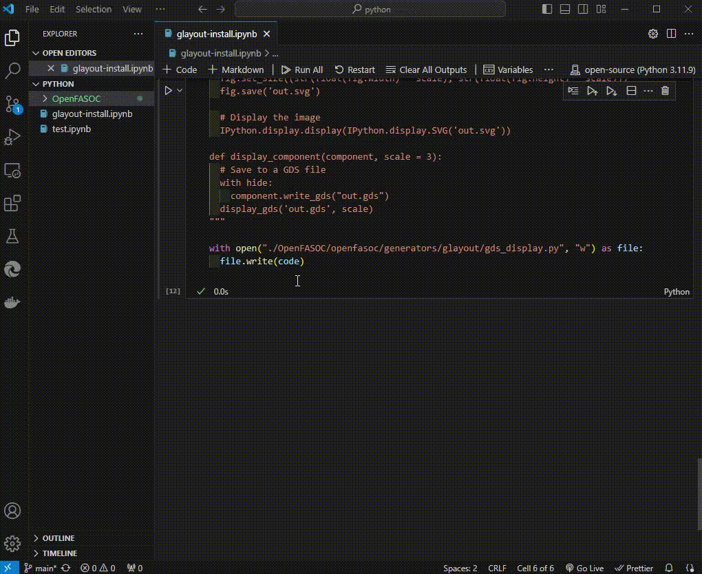
with open("./OpenFASOC/openfasoc/generators/glayout/gds_display.py", "w") as file:
file.write(code)
You can check the generated gds_display.py file in ./OpenFASOC/openfasoc/generators/glayout/
Fix the port_utils.py Code
Okay, we are almost there! We have to make a small change in the port_utils.py code, which is located in ./OpenFASOC/openfasoc/generators/glayout/glayout/flow/pdk/util/port_utils.py.
This is because of prettyprinttree package. I am not sure why it is happening, but I could not import prettyprint package on my side , with an error message of ModuleNotFoundError: No module named 'PrettyPrint'. This package is not an essential one to run the glayout, so we can just comment it out.
- go very deep into the path of
./OpenFASOC/openfasoc/generators/glayout/glayout/flow/pdk/util/port_utils.py - comment out the
PrettyPrintpackage part (shortcutCtrl + /) - search for
PrettyPrintTreeand find the active code which is not commented out - comment out
ptpart and its following codes - save it by
Ctrl + S

Alright! Then we are good to go now!
Generate a Via
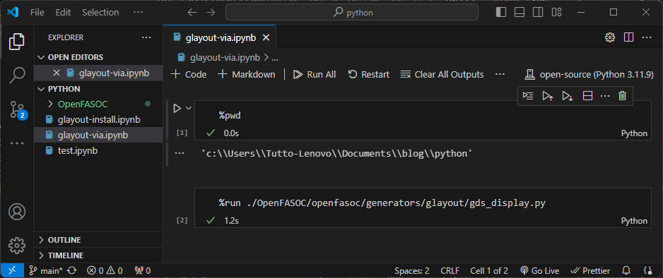
Okay then let’s go through a very simple example of glayout framework, which is generation of a Via.
First of all, make sure you are located in the top-level working directory by running %pwd, in my case it’s python folder. If not, click Restart icon to restart your kernel.
And then run this code to make our gds_display.py code active (see the above screenshot).
%run ./OpenFASOC/openfasoc/generators/glayout/gds_display.py
In this example, 2 files will be generated so let’s make a folder for a tidy arrangement of files.
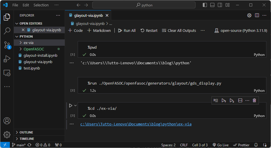
Then, move to our new folder by running %cd ./ex-via and check where you are by running %pwd.
If it was successful, run the following codes one-by-one.
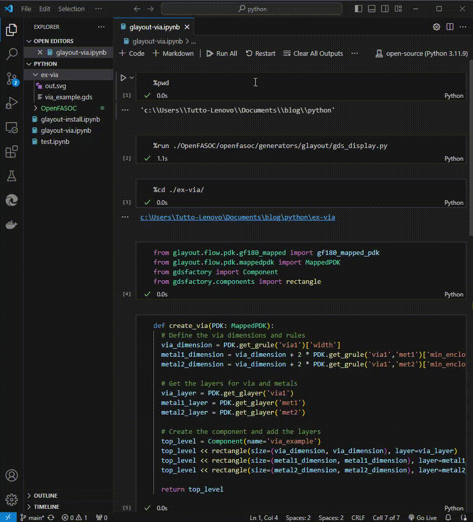
from glayout.flow.pdk.gf180_mapped import gf180_mapped_pdk
from glayout.flow.pdk.mappedpdk import MappedPDK
from gdsfactory import Component
from gdsfactory.components import rectangle
def create_via(PDK: MappedPDK):
  # Define the via dimensions and rules
  via_dimension = PDK.get_grule('via1')['width']
  metal1_dimension = via_dimension + 2 * PDK.get_grule('via1','met1')['min_enclosure']
  metal2_dimension = via_dimension + 2 * PDK.get_grule('via1','met2')['min_enclosure']

  # Get the layers for via and metals
  via_layer = PDK.get_glayer('via1')
  metal1_layer = PDK.get_glayer('met1')
  metal2_layer = PDK.get_glayer('met2')

  # Create the component and add the layers
  top_level = Component(name='via_example')
  top_level << rectangle(size=(via_dimension, via_dimension), layer=via_layer)
  top_level << rectangle(size=(metal1_dimension, metal1_dimension), layer=metal1_layer)
  top_level << rectangle(size=(metal2_dimension, metal2_dimension), layer=metal2_layer)

  return top_level
via_component = create_via(PDK=gf180_mapped_pdk)
via_component.write_gds('via_example.gds')
display_gds('via_example.gds',scale=20)
We generated a Via by only using Python!

Generate a Current Mirror
Similarly, we can also generate a current mirror layout. Like above, follow the below steps.
- Make a Jupyter Notebook file
glayout-mirror.ipynb - Make a new folder
ex-mirror - Move to the new folder by
%cd ./ex-mirror/ - Run the following codes
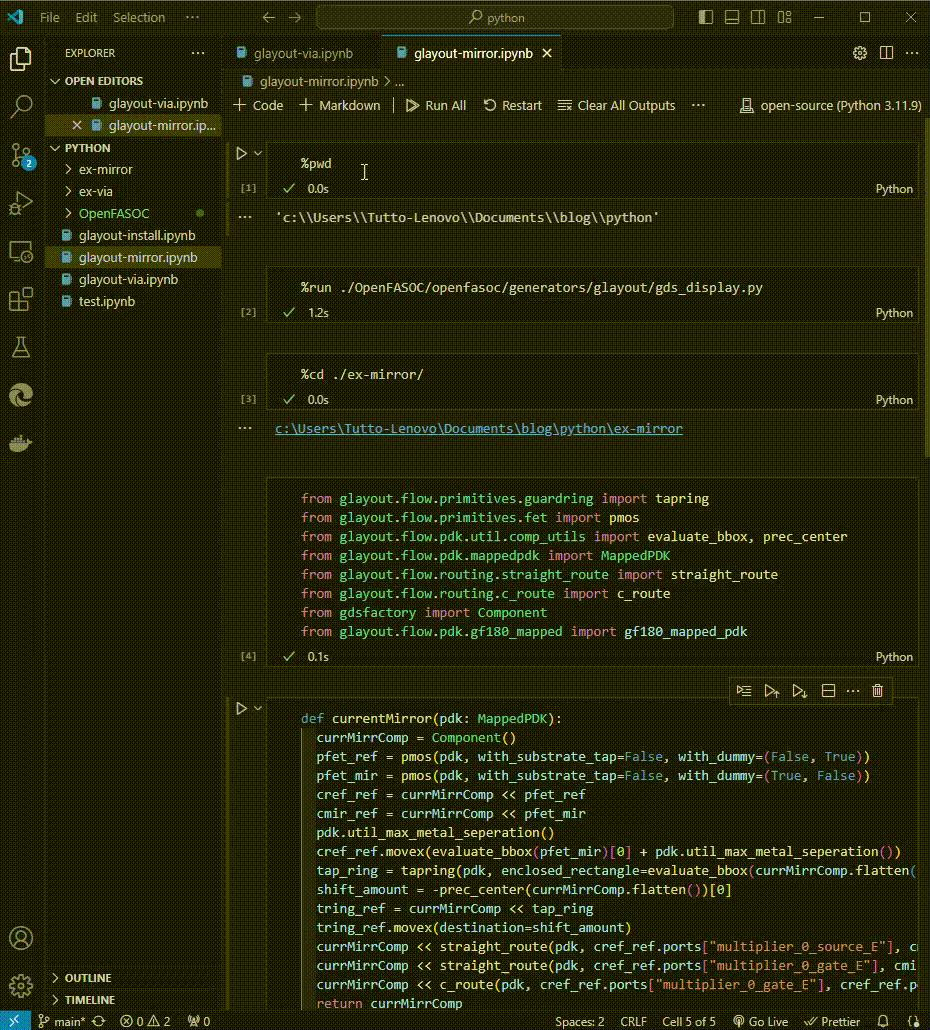
from glayout.flow.primitives.guardring import tapring
from glayout.flow.primitives.fet import pmos
from glayout.flow.pdk.util.comp_utils import evaluate_bbox, prec_center
from glayout.flow.pdk.mappedpdk import MappedPDK
from glayout.flow.routing.straight_route import straight_route
from glayout.flow.routing.c_route import c_route
from gdsfactory import Component
from glayout.flow.pdk.gf180_mapped import gf180_mapped_pdk
def currentMirror(pdk: MappedPDK):
  currMirrComp = Component()
  pfet_ref = pmos(pdk, with_substrate_tap=False, with_dummy=(False, True))
  pfet_mir = pmos(pdk, with_substrate_tap=False, with_dummy=(True, False))
  cref_ref = currMirrComp << pfet_ref
  cmir_ref = currMirrComp << pfet_mir
  pdk.util_max_metal_seperation()
  cref_ref.movex(evaluate_bbox(pfet_mir)[0] + pdk.util_max_metal_seperation())
  tap_ring = tapring(pdk, enclosed_rectangle=evaluate_bbox(currMirrComp.flatten(), padding=pdk.get_grule("nwell", "active_diff")["min_enclosure"]))
  shift_amount = -prec_center(currMirrComp.flatten())[0]
  tring_ref = currMirrComp << tap_ring
  tring_ref.movex(destination=shift_amount)
  currMirrComp << straight_route(pdk, cref_ref.ports["multiplier_0_source_E"], cmir_ref.ports["multiplier_0_source_E"])
  currMirrComp << straight_route(pdk, cref_ref.ports["multiplier_0_gate_E"], cmir_ref.ports["multiplier_0_gate_E"])
  currMirrComp << c_route(pdk, cref_ref.ports["multiplier_0_gate_E"], cref_ref.ports["multiplier_0_drain_E"])
  return currMirrComp

currentMirror(gf180_mapped_pdk).write_gds("cmirror_example.gds")
display_gds("cmirror_example.gds")
Generate Analog Primitives
We can also generate some transistor-level primitive cells for analog circuits, using glayout.
- nmos/pmos
- mimcap
- guardring
- differential pair
- etc
Let’s go through the codes one-by-one.
- Make a Jupyter Notebook file
glayout-prims.ipynb - Make a new folder
ex-prims - Move to the new folder by
%cd ./ex-prims/ - Run the following codes
(Here, I made small changes ofdisplay_componentcode from the originalglayoutexample, to make sure the gds image shows up. You can just copy and paste the codes given in this post)
NMOS
from glayout.flow.primitives.fet import nmos
# Used to display the results in a grid (notebook only)
left = widgets.Output()
leftSPICE = widgets.Output()
grid = widgets.GridspecLayout(1, 2)
grid[0, 0] = left
grid[0, 1] = leftSPICE
display(grid)
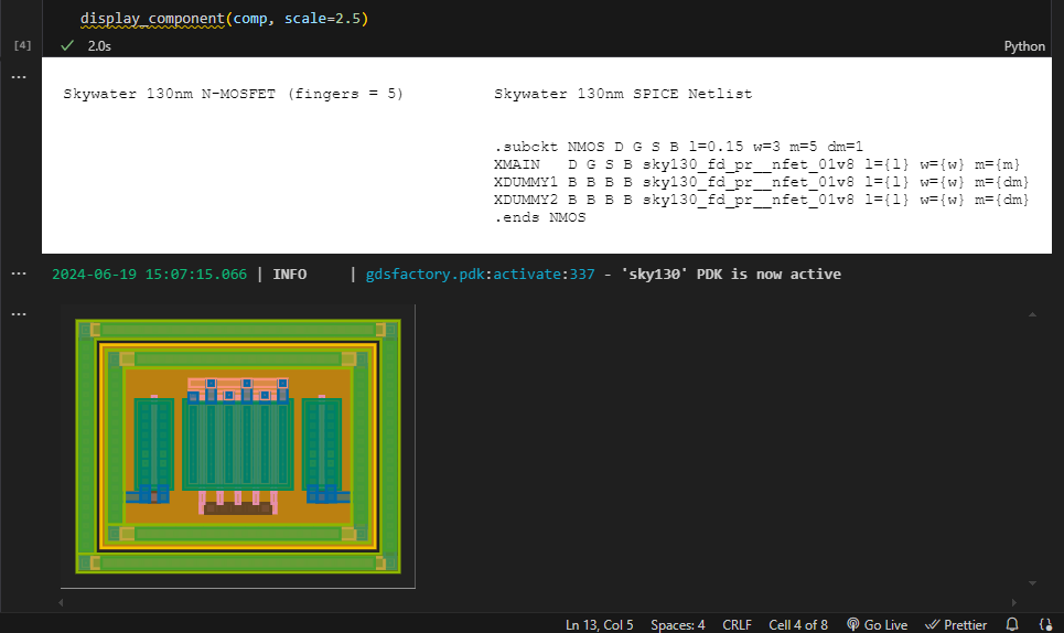
comp = nmos(pdk = sky130, fingers=5)
# Display the components' GDS and SPICE netlists
with left:
print('Skywater 130nm N-MOSFET (fingers = 5)')
with leftSPICE:
print('Skywater 130nm SPICE Netlist')
print(comp.info['netlist'].generate_netlist())
display_component(comp, scale=2.5)
MIM Capacitor
from glayout.flow.primitives.mimcap import mimcap
# Used to display the results in a grid (notebook only)
left = widgets.Output()
leftSPICE = widgets.Output()
grid = widgets.GridspecLayout(1, 2)
grid[0, 0] = left
grid[0, 1] = leftSPICE
display(grid)
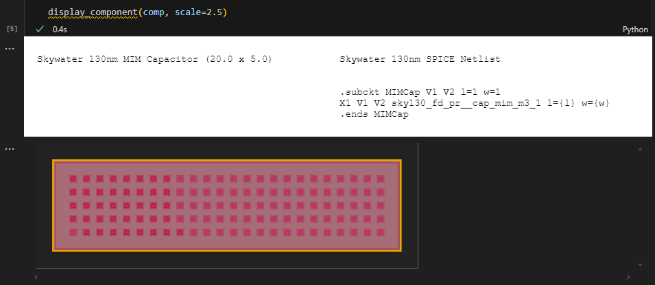
comp = mimcap(pdk=sky130, size=[20.0,5.0])
# Display the components' GDS and SPICE netlists
with left:
print('Skywater 130nm MIM Capacitor (20.0 x 5.0)')
with leftSPICE:
print('Skywater 130nm SPICE Netlist')
print(comp.info['netlist'].generate_netlist())
display_component(comp, scale=2.5)
Guard Ring
from glayout.flow.primitives.guardring import tapring
# Used to display the results in a grid (notebook only)
left = widgets.Output()
leftSPICE = widgets.Output()
grid = widgets.GridspecLayout(1, 2)
grid[0, 0] = left
grid[0, 1] = leftSPICE
display(grid)
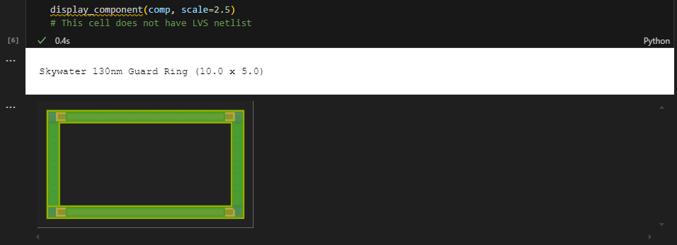
comp = tapring(pdk=sky130, enclosed_rectangle=[10.0, 5.0])
# Display the components' GDS and SPICE netlists
with left:
print('Skywater 130nm Guard Ring (10.0 x 5.0)')
display_component(comp, scale=2.5)
# This cell does not have LVS netlist
Differential Pair
from glayout.flow.blocks.diff_pair import diff_pair
# Used to display the results in a grid (notebook only)
left = widgets.Output()
leftSPICE = widgets.Output()
grid = widgets.GridspecLayout(1, 2)
grid[0, 0] = left
grid[0, 1] = leftSPICE
display(grid)
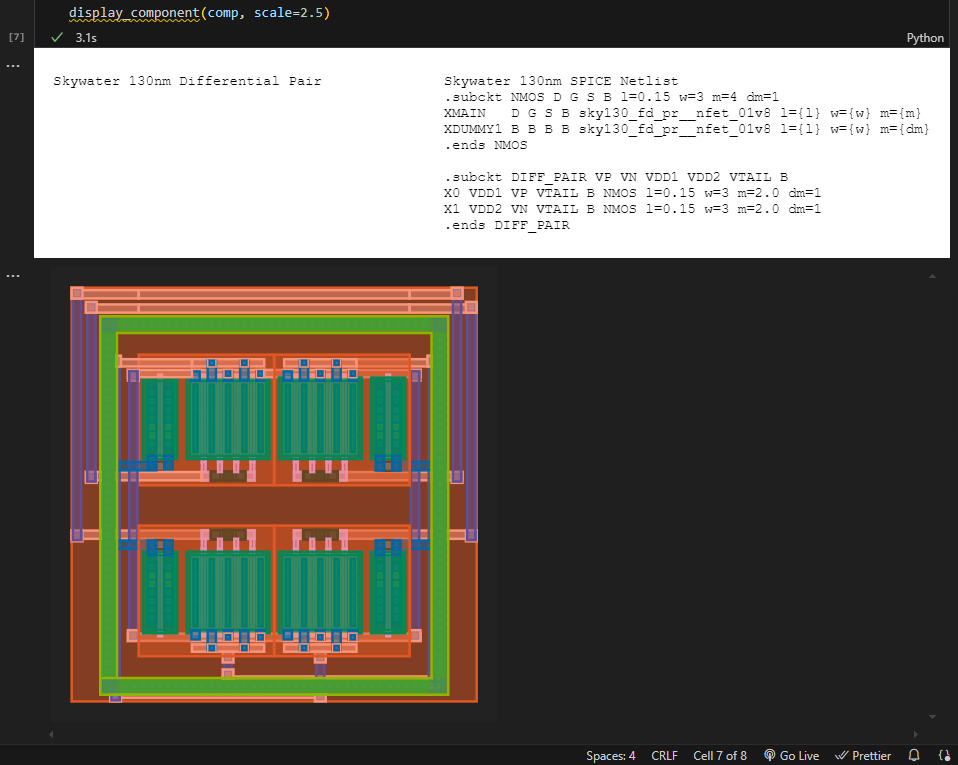
comp = diff_pair(pdk=sky130)
# Display the components' GDS and SPICE netlists
with left:
print('Skywater 130nm Differential Pair')
with leftSPICE:
print('Skywater 130nm SPICE Netlist')
print(comp.info['netlist'].generate_netlist())
display_component(comp, scale=2.5)
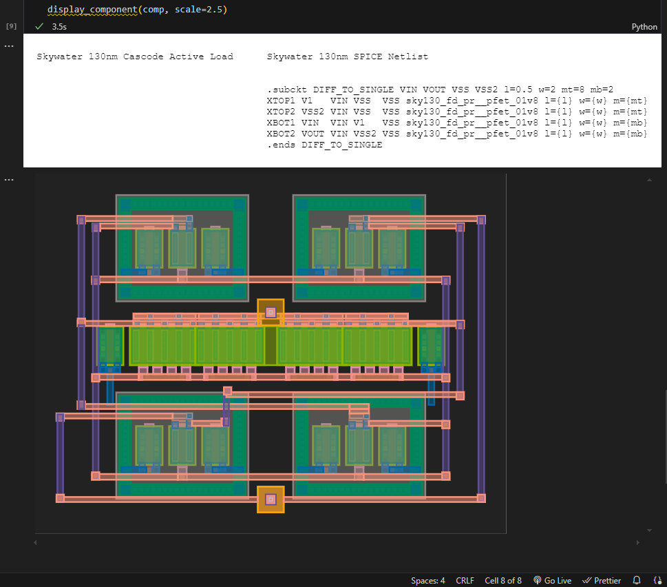
Active Load
from glayout.flow.blocks.differential_to_single_ended_converter import differential_to_single_ended_converter
# Used to display the results in a grid (notebook only)
left = widgets.Output()
leftSPICE = widgets.Output()
grid = widgets.GridspecLayout(1, 2)
grid[0, 0] = left
grid[0, 1] = leftSPICE
display(grid)

comp = differential_to_single_ended_converter(pdk=sky130, rmult=1, half_pload=[2,0.5,1], via_xlocation=0)
# Display the components' GDS and SPICE netlists
with left:
    print('Skywater 130nm Cascode Active Load')
with leftSPICE:
    print('Skywater 130nm SPICE Netlist')
    print(comp.info['netlist'].generate_netlist())

display_component(comp, scale=2.5)
Generate OTA
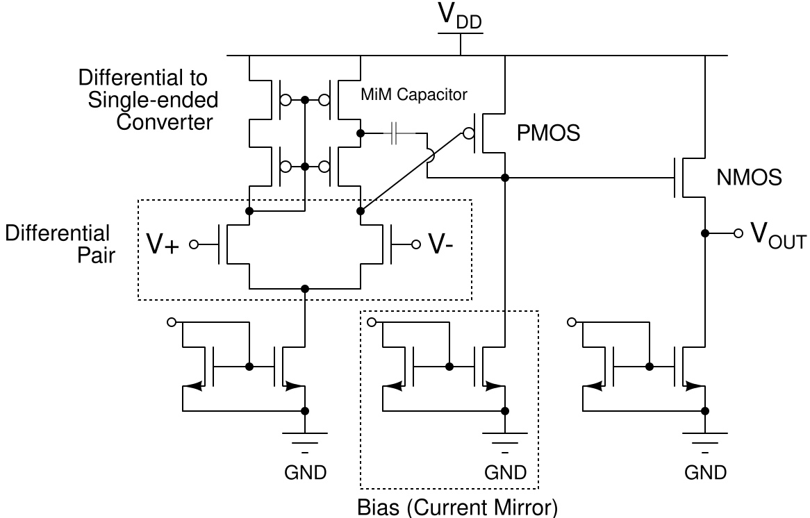
Lastly, let’s try out converting this OTA schematic into layout!
Although it is described as Operational Amplifier (OpAmp) in glayout, technically to say it is more correct to call it Operational Transconductance Amplifier (OTA) since it does not have a low-impedance output stage.
Anyway, you can go through the following steps and generate your OTA.
- Make a Jupyter Notebook file
glayout-ota.ipynb - Make a new folder
ex-ota - Move to the new folder by
%cd ./ex-ota/ - Run the following codes
from glayout.flow.blocks.opamp import opamp
# Select which PDK to use
pdk = sky130
# pdk = gf180
# Op-Amp Parameters
half_diffpair_params = (6, 1, 4)
diffpair_bias = (6, 2, 4)
half_common_source_params = (7, 1, 10, 3)
half_common_source_bias = (6, 2, 8, 2)
output_stage_params = (5, 1, 16)
output_stage_bias = (6, 2, 4)
half_pload = (6,1,6)
mim_cap_size = (12, 12)
mim_cap_rows = 3
rmult = 2
hide = widgets.Output()
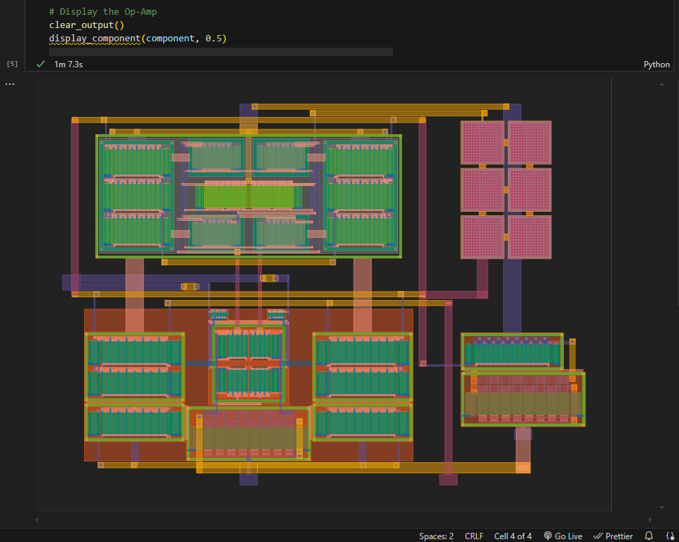
# Generate the Op-Amp
print('Generating Op-Amp...')
with hide:
component = opamp(pdk, half_diffpair_params, diffpair_bias, half_common_source_params, half_common_source_bias, output_stage_params, output_stage_bias, half_pload, mim_cap_size, mim_cap_rows, rmult)
# Display the Op-Amp
clear_output()
display_component(component, 0.5)

Work with Docker
It is also possible to view your layout using open-source design tools!
As described in This Post, we can open the open-source tools as like native applications installed in our OS, using X11 Forwarding and Docker.
Like above, you can set your working directory which will be automatically mounted within Docker. Use klayout and open your generated OTA layout!